Inner Workings of Atomically Thin Transistors
Scientists reveal conductive edges and thread-like flaws using a specialized imaging technique of interest for next-generation electronics.

The Science
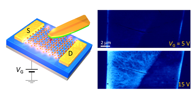
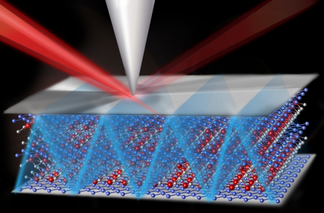
To build better computer chips in the future, researchers are exploring devices built on atomically thin, two-dimensional materials such as molybdenum disulfide (MoS2). These devices are the basic elements for the on and off switches for computer processing. Scientists at the University of Texas at Austin devised an imaging tool. It visualizes the distribution of electrical conductance during the normal operation of MoS2 transistors. In doing so, the team found one-dimensional conductive edges. These edges may carry enough current for functional devices. They also revealed flaws that need to be eliminated in future material preparations and device fabrication.
The Impact
Devices based on high-quality materials with novel functions, beyond those in use today, are desired for next-generation electronics and photonics. Peering into the active devices while they operate can provide critical insight for further improvements of the material quality and device processing. Taking advantage of the newly discovered conductive edges, it may be possible to only use these one-dimensional channels and substantially reduce the power loss in transistors.
Summary
The understanding of microscopic properties of atomically thin materials, such as molybdenum disulfide (MoS2), is of fundamental importance for application of this class of materials (transition-metal dichalcogenides) in electronics and photonics. Because of various imperfections at the edges and interior of these atomically thin sheets, electrons moving on the atomic planes experience spatially nonuniform electric fields, whose effect on the charge transport has not been fully studied. Using a specialized technique known as near-field scanning microwave impedance microscopy, scientists at the University of Texas at Austin peered into a working MoS2 field-effect transistor with the same device configuration as the building blocks in our computer chips. Interestingly, as the devices were gradually turned on, electrical conduction began at the edges of the atomic sheets before appearing in the interior. They explained the results by theoretical calculations that take the atomic configurations at the edges into account. With further improvement of the material quality, these one-dimensional channels may even carry sufficient current to substantially reduce the power loss in future devices. Scientists will need to minimize the defects in the material, which manifest themselves as thread-like features with lower conductance than the background in the microwave images, for future material preparations and device fabrications. The simultaneous device operation and local imaging experiments pave the way for both fundamental research and practical applications on these fascinating materials.
Contact
Keji Lai
University of Texas at Austin
kejilai@physics.utexas.edu
Funding
The microwave imaging of the materials was supported by the U.S. Department of Energy (DOE), Office of Science, Basic Energy Sciences, under an Early Career Award. The device fabrication was partially supported by the Welch Foundation and Office of Naval Research and Nanomanufacturing Systems for Mobile Computing and Energy Technologies (NASCENT) Engineering Research Center. Theoretical calculations were supported by China 973 Program, DOE, and the Welch Foundation.
Publications
D. Wu, X. Li, L. Luan, X. Wu, W. Li, M.N. Yogeesh, R. Ghosh, Z. Chu, D. Akinwande, Q. Niu, and K. Lai, “Uncovering edge states and electrical inhomogeneity in MoS2 field-effect transistors.” Proceedings of the National Academy of Sciences USA 113, 8583-8588 (2016). [DOI: 10.1073/pnas.1605982113]
Related Links
University of Texas news: Scientists Glimpse Inner Workings of Atomically Thin Transistors
AzoNano article: Physicists Get First Glimpse of Inner Workings of Atomically Thin Semiconductor Devices
Highlight Categories
Performer: University
Additional: Technology Impact , Collaborations , Non-DOE Interagency Collaboration , International Collaboration


