Connecting Three Atomic Layers Puts Semiconducting Science on Its Edge
New material with a layered, atomic sandwich structure has unique optoelectronic properties.

The Science
A new semiconducting material that is only three atomic layers thick that exhibits electronic properties beyond traditional semiconductors has been developed. Two nano-engineered configurations of the material have shown an enhanced response to light.
The Impact
Layered materials at the atomic limit, where electrons are constrained to two dimensions, can be engineered into electronic structures with unique optical, electronic, and magnetic properties. The new structures are a test bed for theories of low dimensional materials physics, but more practically, the optical manipulation of electron charge and magnetic order can lead to new modes of solar energy conversion and flexible, transparent computation devices.
Summary
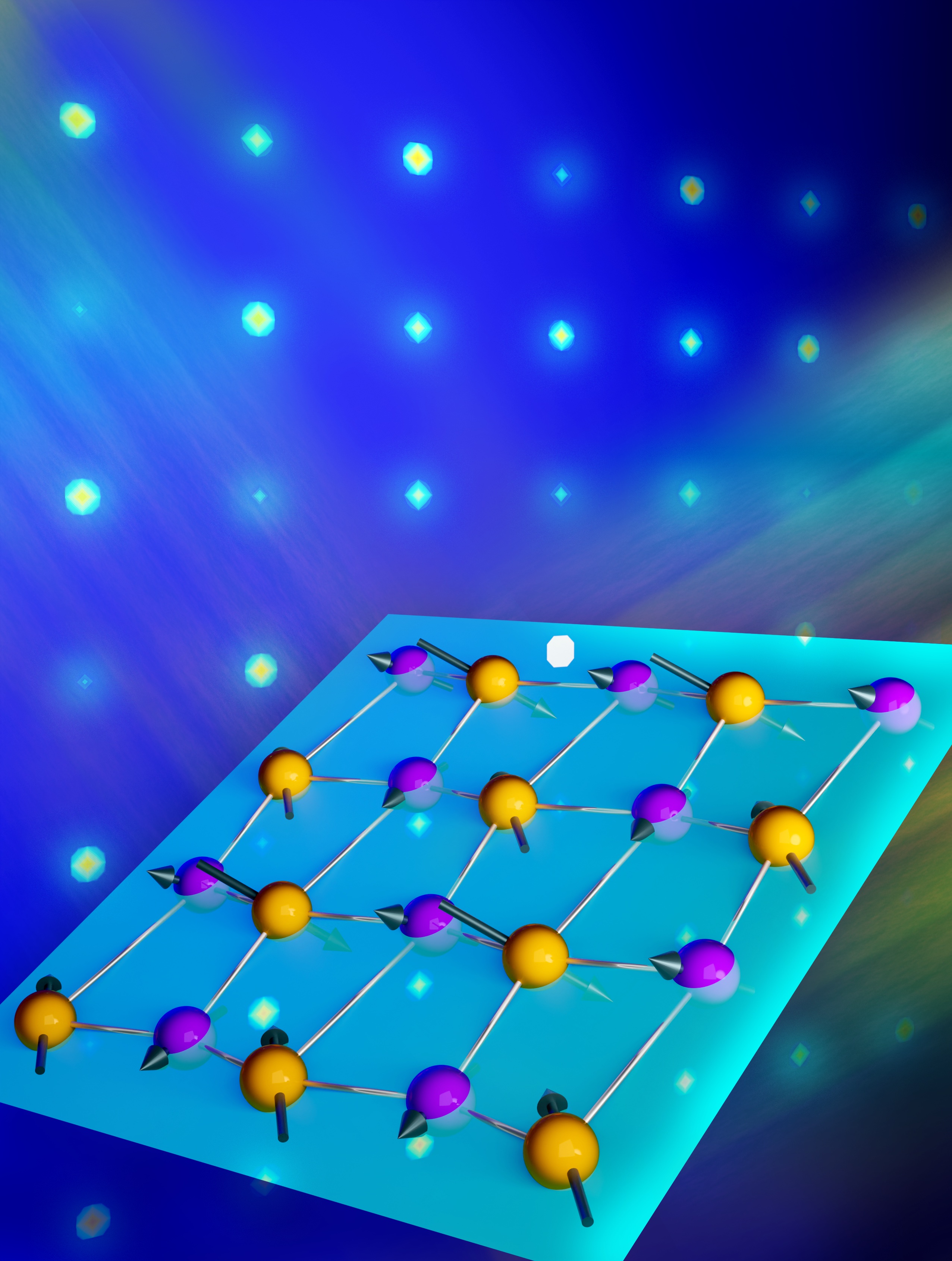
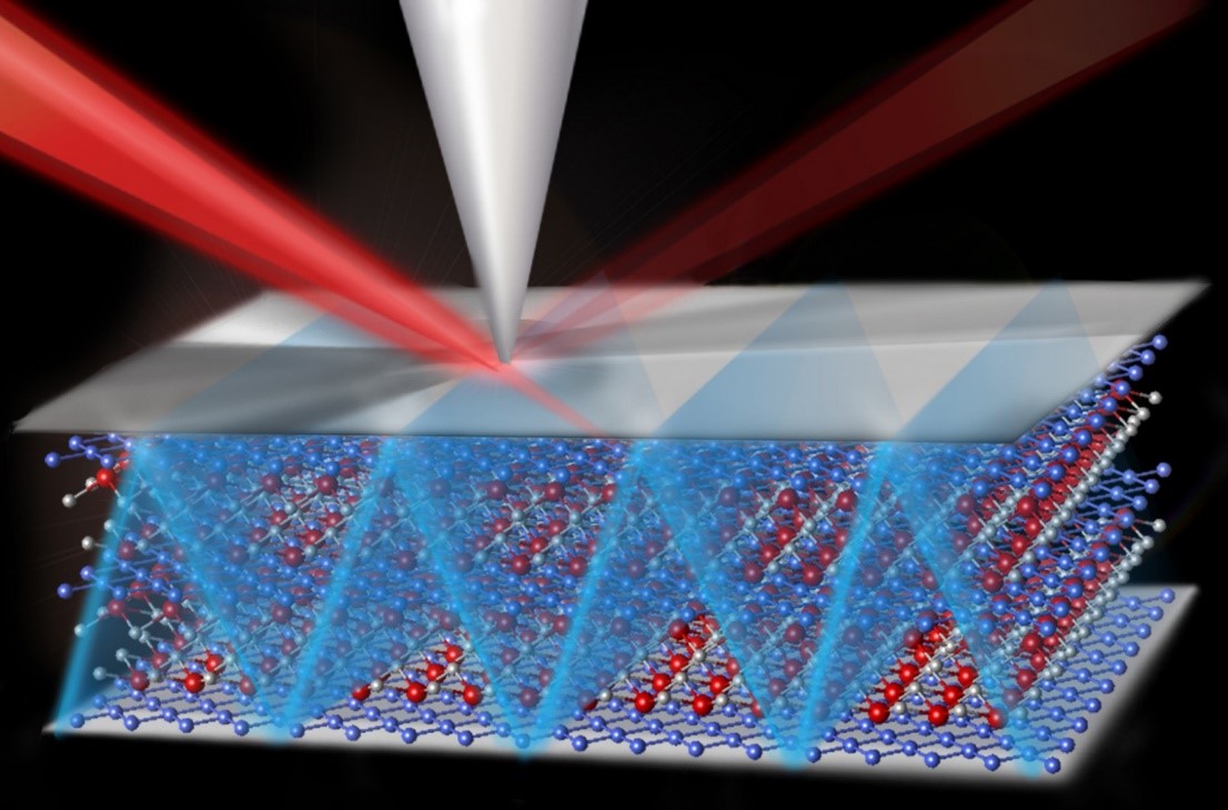
A new ultra-thin semiconducting material consists of three atomic layers in an “atomic sandwich” configuration with a heavy metal atom layer between two selenium layers. The material is quasi-two dimensional, just three atoms thick, and exhibits unique properties at junctions. When the material is exposed to light and absorbs photons, excited electrons are created which remain coherently coupled, in unique ways, with the charge “hole” they left behind. Stacking up tow “atomic sandwiches” yields coupled excited charge states across the planar interface with the magnetic direction or “spin state” becoming aligned for a large population of electrons. A companion result by the same research group demonstrated a method to make the edge of one metal layer match up with the edge of a second, different metal layer – a linear boundary or “hetero-junction” rather than the more typical planar boundary. Engineered electron spin and charge polarization, as well as transport across or along the interface, might be possible as evidenced by the enhanced photoluminescence signals at these positions.
Contact
Xiaodong Xu
University of Washington
xuxd@uw.edu
Funding
Primary support by the DOE Office of Science, Basic Energy Sciences. Some students were supported by graduate student fellowships and doctoral training grants (NSF, EPSRC, HEFCE, and Cottrell Scholar Award). Some researchers were supported by the Hong Kong Research Grant Council, the Croucher Foundation, the Science City Research Alliance and the University of Washington Clean Energy Institute.
Publications
A.M. Jones, H. Yu, J.S. Ross, P. Klement, N.J. Ghimire, J. Yan, D.G. Mandrus, W. Yao, X. Xu, “Spin-layer locking effects in optical orientation of exciton spin in bilayer WSe2,” Nature Physics 10, 130–134, 2014. [DOI: 10.1038/nphys2848]
C. Huang, S. Wu, A.M. Sanchez, J. J.P. Peters, R. Beanland, J.S. Ross, P. Rivera, W. Yao, D.H. Cobden, X. Xu, “Lateral heterojunctions within monolayer MoSe2–WSe2 semiconductors,” Nature Materials 13, 1096–1101, 2014. [DOI: 10.1038/NMAT4064]
Related Links
Highlight Categories
Additional: Collaborations , Non-DOE Interagency Collaboration