Towards Understanding Electronic Switching in Magnets
Researchers have invented a new x-ray imaging technique that could reveal key atomic-scale properties in ferroelectric magnetic materials.

The Science
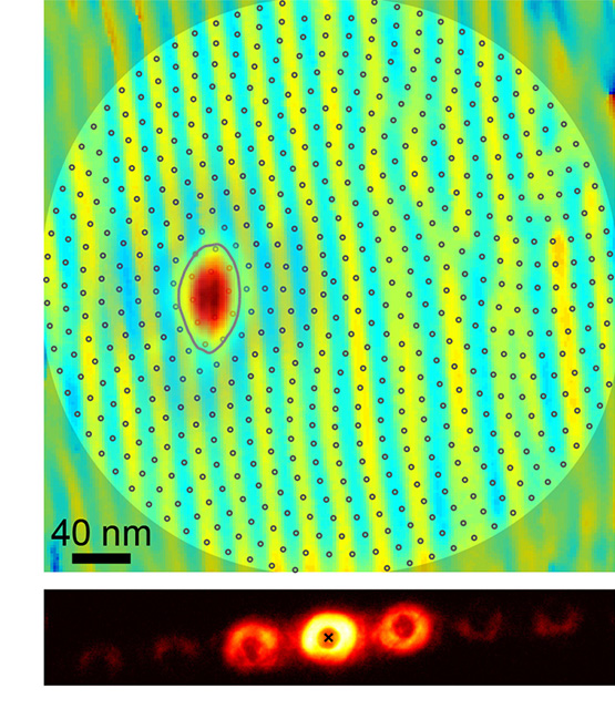
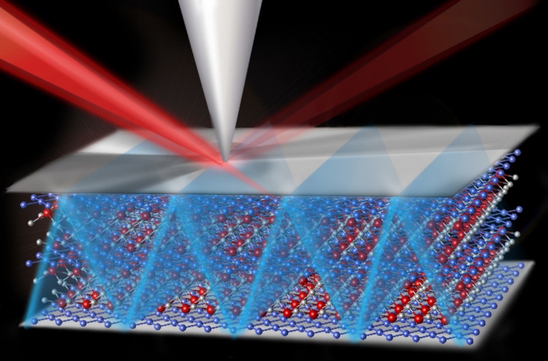
Ferroelectric materials are found in a wide range of technologies including medical imaging, infrared cameras, and sensors. Core to the special properties of these materials are atomic regions, or domains, with localized alignments of charges that often occur as stripes. Using an x-ray technique called “Bragg Projection Ptychography,” the ferroelectric domains were characterized by combining a series of x-ray scattering patterns from a synchrotron x-ray beam. This technique can investigate the ferroelectric material in realistic device architectures - even during the fabrication process.
The Impact
This new penetrating, non-destructive and high resolution x-ray imaging technique can be used to study the behavior of ferroelectric materials during the harsh conditions of film growth or to characterize the material below the coatings used in energy conversion devices. The improved resolution and size of the image provides a unique opportunity to understand and engineer the domain regions that control the electronic properties in magnetic and charge-aligned thin film materials.
Summary
Crystalline materials scatter x-rays and encode a structural signature of the atomic positions into the diffracted x-ray beam. Somewhat like the images from a CAT scan used in medical procedures, a recently developed technique continuously stitches together nano-beam diffraction patterns taken in an overlapping array of sampling points. In the present case, the data yields an image that is sensitive to the charge distortion in a ferroelectric thin film, a material with regions of polarized electronic charge (called domains) that is used in a wide range of devices. The result is a map with a resolution of 6 nanometers (few atomic cells of the material), sufficient to study domain wall arrangements and manipulation. This high resolution is enabled by modern synchrotron x-ray sources that have x-ray beams with laser-like, well-defined, coherent wave shapes. A computer algorithm was used to refine the x-ray scattering data into high-resolution structural maps. The technique has been shown to be sensitive to ferroelectric charge distortions that are fractions of an atomic spacing in size. The x-ray result does not require contact with the material and is consistent with images observed with contact scanning force microscopy. The x-ray technique can also be used to probe material found in buried device-like architectures and in complex chemical environments.
Contact
Paul Fuoss
Argonne National Laboratory
Fuoss@anl.gov
Funding
Department of Energy, Office of Science, Basic Energy Sciences program, for both the research and the use of the Advanced Photon Source and Center for Nanoscale Materials user facilities at ANL.
Publications
S. O. Hruszkewycz, M. J. Highland, M.V. Holt, Dongjin Kim, C. M. Folkman, Carol Thompson, A. Tripathi, G. B. Stephenson, Seungbum Hong, and P. H. Fuoss, Phys. Rev. Lett. 110, 177601 (2013).
Highlight Categories
Performer: DOE Laboratory , SC User Facilities , BES User Facilities , APS , CNM


