Hundred-Fold Improvement in Temperature Mapping Reveals the Stresses Inside Tiny Transistors
New nanoscale thermal imaging technique shows heat building up inside microprocessors, providing new information to help solve heat-related performance issues.

The Science
A team of users and staff working at the Molecular Foundry have created a thermal imaging technique that can “see” how temperature changes from point to point inside the smallest electronic circuits.
The Impact
Used in everything from cell phones to supercomputers, modern microelectronic circuits contain billions of nanometer-scale transistors, each generating tiny amounts of heat that collectively can compromise the performance of the device. Seeing where the heat is generated provides valuable information for circuit designers to probe where failures are occurring and to realize the next generation microprocessors.
Summary
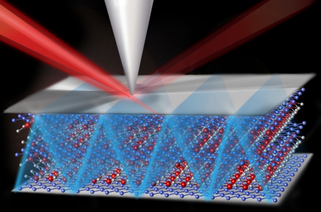
Electrons passing through a sample excite collective charge oscillations called plasmons. Monitoring the energy required to excite the plasmons enables measuring local variations in a sample’s density, which are directly related to the local temperature within an integrated circuit or transistor. Based on these principles, the researchers developed a new technique called plasmon energy expansion thermometry, or PEET. It enables measuring local temperature with 3-5 K precision and 5 nm spatial resolution. The new technique provides 100-fold better resolution than optical pyrometry. The new technique is the only technique that allows correlation of atomically resolved structure to a device’s thermal characteristics.
Contact
Shaul Aloni
The Molecular Foundry, LBNL
saloni@lbl.gov
(510) 486-7452
Funding
This work has been supported by National Science Foundation award DMR-1206849 and in part by Function Accelerated nanoMaterial Engineering (FAME), one of six centers of Semiconductor Technology Advanced Research network (STARnet), a Semiconductor Research Corporation program sponsored by the Microelectronics Advanced Research Corporation and Defense Advanced Research Projects Agency. Data presented in this article were acquired at the Center for Electron Microscopy and Microanalysis at the University of Southern California. Work at the Molecular Foundry was supported by the Office of Science, Office of Basic Energy Sciences, of the U.S. Department of Energy under contract DE-AC02-05CH11231.
Publications
M. Mecklenburg, W. A. Hubbard, E. R. White, R. Dhall, S. B. Cronin, S. Aloni, and B. C. Regan, “Nanoscale temperature mapping in operating microelectronic devices.” Science 347 6222 (2015). [DOI: 10.1126/science.aaa2433.]
Related Links
Microscopy and Analysis Article
Royal Society of Chemistry Article
Highlight Categories
Performer: SC User Facilities , BES User Facilities , Foundry
Additional: Technology Impact , Collaborations , Non-DOE Interagency Collaboration