Patterning Silicon at the One Nanometer Scale
Scientists engineer materials’ electrical and optical properties with plasmon engineering
The Science
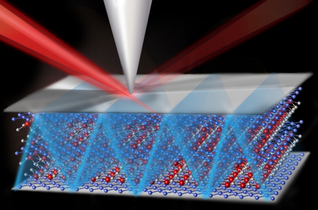
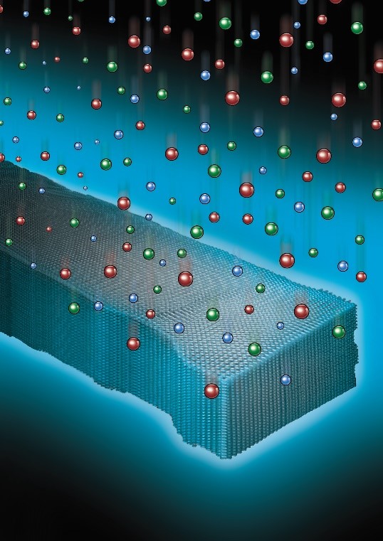
Researchers have developed an innovative technique for creating nanomaterials. These are materials only atoms wide. They draw on nanoscience to allow scientists to control their construction and behavior. The new electron beam nanofabrication technique is called plasmon engineering. It achieves unprecedented near-atomic scale control of patterning in silicon. Structures built using this approach produce record high tuning of electro-optical properties.
The Impact
In this research, scientists used plasmon engineering to control the optical and electronic properties of silicon. The technique uses aberration-corrected electron beam lithography. This process involves using a beam of electrons to modify the surface of a material. Plasmon engineering allowed researchers to modify material at the near atomic scale. The use of “conventional” lithography means this approach could one day be applied to industrial applications. This approach will benefit researchers working on optical communications, sensing, and quantum computing.
Summary
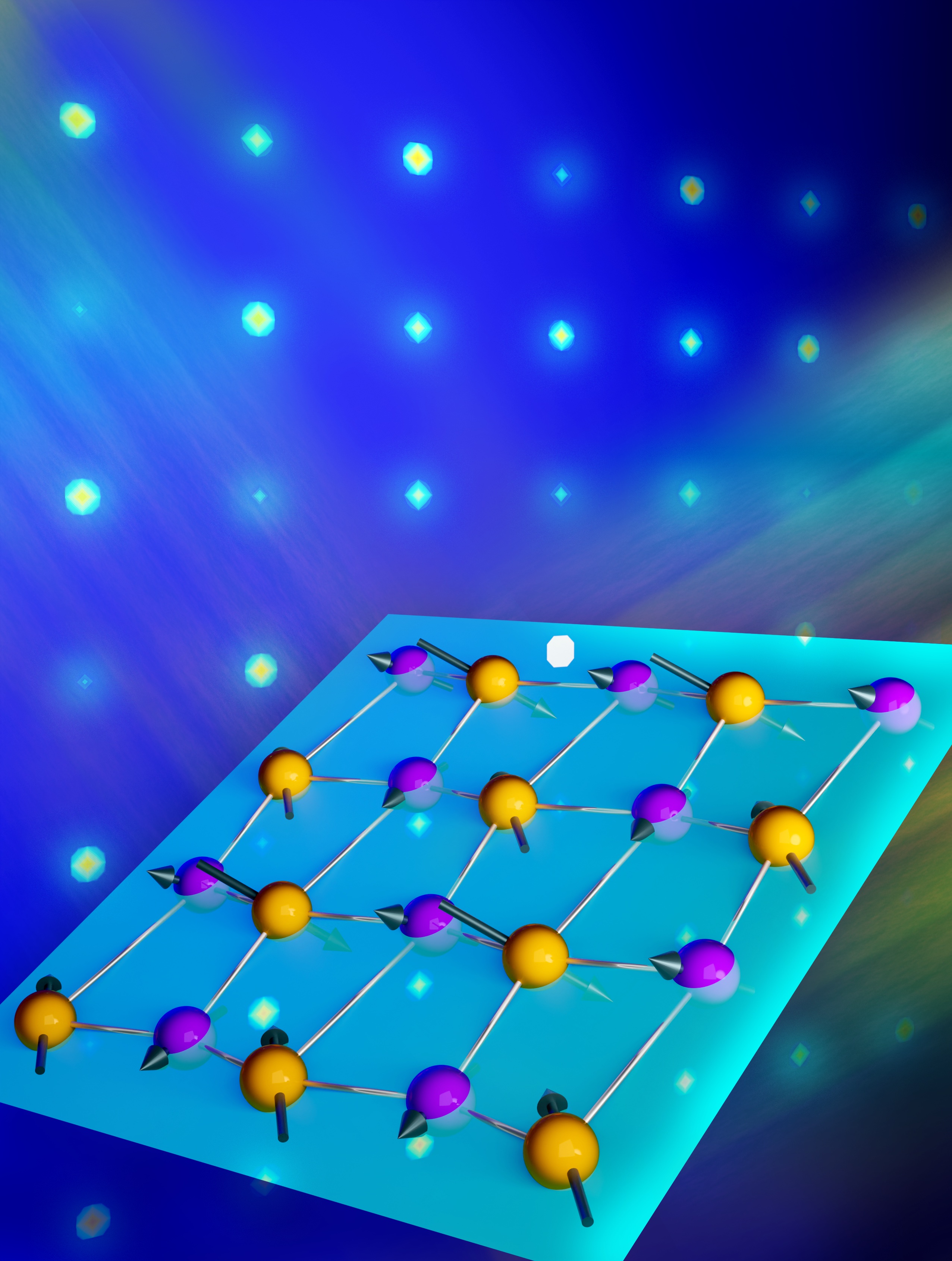
Patterning materials at single nanometer resolution allows scientists to precisely engineer quantum confinement effects. Quantum effects are significant at these length scales and controlling the nanostructure dimensions provides direct control over electrical and optical properties. Silicon is by far the most widely-used semiconductor material in electronics, and the ability to fabricate silicone‐based devices of the smallest dimensions for novel device engineering is highly desirable. Researchers at Brookhaven’s Center for Functional Nanomaterials, a Department of Energy user facility, used aberration‐corrected electron‐beam lithography combined with dry reactive ion etching to achieve patterning of 1 nanometer features as well as surface and volume plasmon engineering in silicon. The nanofabrication technique employed here produces nanowires with a line edge roughness of 1 nanometer. In addition, this work demonstrates tuning of the silicon volume plasmon energy by 1.2 electron volt from the bulk value, which is ten times higher than previous attempts of volume plasmon engineering using lithographic methods.
Contact
Fernando Camino
Center for Functional Nanomaterials
fcamino@bnl.gov
Funding
This research was supported by the DOE Office of Science and used resources at the Center for Functional Nanomaterials, an Office of Science user facility at Brookhaven National Laboratory.
Publications
Manfrinato, V.R., et al., Patterning Si at the 1 nm Length Scale with Aberration-Corrected Electron-Beam Lithography: Tuning of Plasmonic Properties by Design, Advanced Functional Materials 1903429 (2019). [DOI: 10.1002/adfm.201903429]
Highlight Categories
Program: SUF
Performer: DOE Laboratory , CFN