How to 3D Print on the Nanoscale
Electron beam controllably builds micro- and nanoscale structures, enabling new three-dimensional materials.

The Science
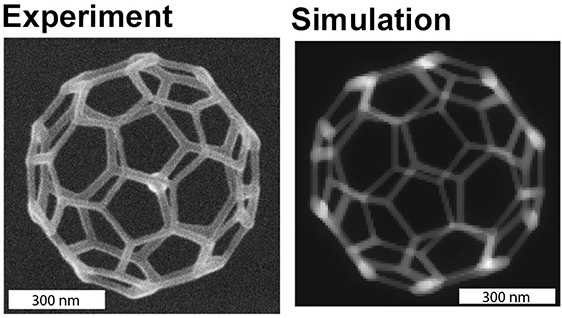
Realization of “3D printing” material assembly on the micron or even nanometer scale has posed significant challenges to researchers. Now, scientists have developed a specialized computer simulation that guides an electron beam to create custom 3D structures. The beam induces a precursor material to deposit in a way that forms complex shapes. This nanoscale 3D printing creates freestanding structures so tiny that bacteria dwarf them.
The Impact
The new approach, simulation-guided material deposition at the nanoscale, offers a path to synthesize materials with superior mechanical and optical properties. This design approach replaces trial-and-error in nanomanufacturing for materials and structures with superior mechanical and optical properties.
Summary
Precision control of nanometer scale 3D fabrication has been a longstanding research goal. Now, researchers have developed a 3D simulation that guides focused electron beam induced deposition (FEBiD) of precursor molecules on a surface and accurately predicts the complex geometries of deposited shapes over the length scale from nanometers to micrometers. The simulation predicts gas-solid interactions where the electron beam strikes a surface. While FEBiD can direct-write freestanding 3D nanostructures, improved understanding of the dynamic interplay of the scanning electron beam and adsorbed precursor molecules is critical for advancing additive manufacturing of optoelectronics, metamaterials, and more. The simulations consist of (1) a Monte Carlo simulation to calculate the electron–solid interaction and (2) a continuum simulation to calculate surface adsorption, desorption, diffusion, and deposition of precursor molecules. The merged simulation can guide the electron beam to produce complex lattices and meshes sized between 10 nanometers and 1 micron.
Contact
Jason Fowlkes
Center for Nanophase Materials Sciences
Oak Ridge National Laboratory
fowlkesjd@ornl.gov
Funding
The Oak Ridge National Laboratory portion of this research was supported by the Center for Nanophase Material Sciences, a U.S. Department of Energy Office of Science user facility. Individual researchers received support from Chemistry for ELectron-Induced NAnofabrication (CELINA) COST Action CM1301, EUROSTARS project TRIPLE-S, the BMVIT exchange program (through Austria’s Ministry of Transport, Innovation and Technology), the National Defense Science and Engineering Graduate Fellowship funded through the Air Force Office of Scientific Research, and the University of Tennessee Chancellor’s Fellowship program.
Publications
J. Fowlkes, R. Winkler, B.B. Lewis, M.G. Stanford, H. Plank, and P.D. Rack, “Simulation guided 3D nanomanufacturing via focused electron beam induced deposition.” ACS Nano 10, 6163-6172 (2016). [DOI: 10.1021/acsnano.6b02108]
Related Links
Oak Ridge National Laboratory press release: Researchers combine simulation, experiment for nanoscale 3-D printing
Highlight Categories
Performer: University , DOE Laboratory , SC User Facilities , BES User Facilities , CNMS
Additional: Collaborations , Non-DOE Interagency Collaboration


