Working Better Together: Two Materials Defining the Future of High-Speed Electronics
Junctions between conductive graphene and insulating nanotubes could lead to faster electronics and computers.
The Science
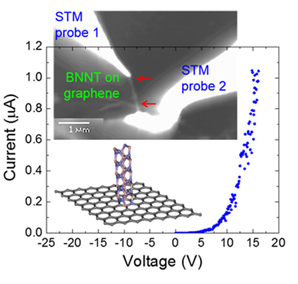
Computers and electronics rely on heterojunctions, which are the interfaces between two different materials with different electronic properties, typically two semiconducting materials. In this research, scientists achieved seamless heterojunctions of graphene-boron nitride nanotubes without using conventional semiconductors. Further, they experimentally found the junctions behaved as electronic switches. The on/off “switching ratio” was as high as 100,000, which is several orders of magnitude higher than current graphene switches.
The Impact
The high on/off switching ratio of these tiny heterojunctions could lead to developing high-speed electronic switches that overcome conventional material constraints and lead to faster electronics and computers.
Summary
Towards the development of high-speed electronic devices that are usually constrained to conventional semiconductors, researchers led by Michigan Technological University have discovered a novel semiconducting device using a conductive graphene sheet and an insulating boron nitride (BN) nanotube. Researchers discovered that the point of contact between the single-atom-thick graphene sheet and the BN nanotube produced a remarkable heterojunction. Electrons move quickly in the conductive graphene, but are halted by the wide bandgap of the BN nanotube. The nanometer-sized barrier prevents current from flowing across the junction. This lack of current flow can be overcome by applying voltage. During real-time imaging, a four-probe scanning tunneling microscope was used to determine the switching ratio (ratio of current flow with the field “on” to with the field “off”). Impressively, the switching ratio was 100,000. Theoretical calculations suggest that the switching behavior is due to a mismatch of the density of available energy states between the graphene and the BN nanotube. These switches could lead to the development of high-speed electronic switches, which have applications ranging from digital electronics to computers.
Contact
Yoke Khin Yap
Michigan Technological University
ykyap@mtu.edu
Funding
This work was supported by the U.S. Department of Energy (DOE), Office of Science, Office of Basic Energy Sciences, including support of the Center for Nanophase Materials Sciences and Center for Integrated Nanotechnologies, DOE Office of Science User Facilities; and the U.S. Army Research Laboratory.
Publications
V. Parashar, C. P. Durand, B. Hao, R. G. Amorim, R. Pandey, B. Tiwari, D. Zhang, Y. Liu, A. P. Li, and Y. K. Yap, "Switching behaviors of graphene-boron nitride nanotube heterojunctions." Scientific Reports 5, 12238 (2015). [DOI: 10.1038/srep12238].
Related Links
Highlight Categories
Performer: University , DOE Laboratory , SC User Facilities , BES User Facilities , CINT , CNMS
Additional: Collaborations , Non-DOE Interagency Collaboration