Seeing Matter at Atomic and Molecular Scales
From Nanoscale Structure to Macroscale Properties
How do only 118 building blocks—all the known elements in the periodic table—combine to create every substance on Earth? How do these atoms make materials with a seemingly endless variety of forms and properties—soft and hard, ductile and brittle, magnetic and nonmagnetic, insulating and superconducting, living and nonliving? Why do the same atoms connected in varying ways yield remarkably different materials? Finding out is key to creating the materials and technologies needed to thrive in an age of natural resource, environmental, and fiscal constraints. This quest begins with visualizing atoms (nuclei and electrons) and their interactions.

Download High Resolution Image
Studying matter at the level of atoms and molecules requires measuring structures that are billionths of a meter (nanometers) or less in size. This nanoscale realm is where the fundamental properties of materials are established. Melting temperature, magnetic properties, charge capacity, and even color are dictated by the arrangements of atoms and molecules. The ability to understand, design, and control these properties will lead to a new world of materials and technologies for numerous application areas. An atom’s typical size is tenths of a nanometer. The wavelength range of visible light is a few hundred nanometers, which is too large to detect atoms. Seeing matter at the level of atoms requires instruments that can measure structures that are one thousand times smaller than those detectable by the most advanced light microscopes. Thus, to characterize structures with atomic detail, we must use probes such as x-rays, electrons, and neutrons that are at least as small as the atoms being investigated.
The fundamental tenet of materials research is that structure determines function. Advanced tools based on x-ray, electron, and neutron beams are providing atomic details of metal alloys, plastics, enzymes, superconductors, carbon nanostructures, and materials under extremes of temperature, pressure, and stress. Models and simulations empowered by supercomputers are helping researchers test theories and explore the nanoscale dynamics of materials with greater realism. By advancing our atom-by-atom understanding of material structure, we open up a dazzling array of possibilities for designing new materials with desired properties and functions.
| Front Side | Back Side |
|---|---|
 |
 |
|
11" x 17" Placemat: 300 DPI High-res PDF | 120 DPI Low-res PDF |
|
Carbon: The Many Faces of the Sixth Element
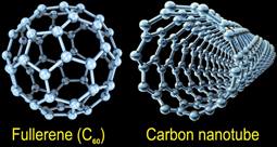
Seemingly minor changes in the positions and connections among atoms can yield materials with very different physical properties. For example, carbon atoms can assemble into diverse structural forms—diamond, graphite and graphene, carbon nanotubes, and fullerenes (buckyballs)—each with unique characteristics. By tapping nature's secrets for building matter atom by atom, nanotechnology researchers can design and build a new generation of nanostructures that outperform existing materials.
In diamond, each carbon atom forms strong covalent bonds with four other carbon atoms, making it the hardest natural substance known. In graphite, many one-atom-thick layers of carbon are held together by weak attractive forces that make it soft and brittle. Spherical fullerenes, cylindrical carbon nanotubes, and graphene sheets are nanomaterials with extraordinary mechanical, chemical, and electronic properties for advanced applications in energy, medicine, computing, and other technologies.
X-Ray Science
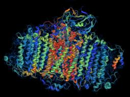
Photosystem I is a complex, membrane-bound molecular machine in plant cells that converts sunlight to energy during photosynthesis. Membrane proteins represent an important class of macromolecules targeted by industrial biotech companies and drug developers.
For nearly a century, x-ray beams have been our principal means of unraveling the identities and positions of atoms in crystallized samples ranging from relatively simple metal materials to highly complex biological molecules like proteins and DNA. Due to their short wavelength, hard x-rays are very useful for probing atomic structure. Today’s synchrotron radiation and free-electron laser light sources produce x-rays so intense that they have vastly eclipsed historical methods and have given rise to scores of new ways to do experiments.
Crystallized samples of materials are analyzed by passing x-rays through them. The x-rays are scattered by the atoms of a crystal, producing a diffraction image on detectors. This image provides unique information on the identity of the atoms and structure of the crystal. Large, flexible membrane proteins, such as Photosystem I in plant cells, form very small crystals that tend to be imperfect and weakly diffracting. Intense x-ray sources have been invaluable for determining the structures and properties of such macromolecules.
Electron Science
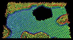
Powerful electron microscopy provides real-time imaging of atoms repositioning themselves along the edge of a hole blown through a sheet of graphene, a one-atom-thick layer of carbon atoms. Understanding stable edge arrangements may hasten development of advanced electronic devices based on carbon’s outstanding electronic and structural properties. The raised features are adsorbed molecules.
Because of the strong interactions between negatively charged electrons and the charged particles in matter, electron beams can provide important structural and chemical information underlying the behavior of various materials. Today’s most advanced electron microscopes can produce electron beams that are so bright they can be used to visualize subnanometer phenomena such as the electronic structure and bonding of atoms. By understanding the atom-by-atom assembly of materials into stable configurations, researchers are gaining new insights into improving existing materials and synthesizing new nanostructures with superior strength, durability, corrosion resistance, and other desired properties.
Neutron Science

A neutron scattering spectrum shows time- and space-dependent magnetic fluctuations in a superconductor. The observed fourfold symmetry of the spin excitations suggests a common origin for superconducting states in different classes of materials.
Unlike x-rays and electron beams that interact with a material’s electrons, neutrons have no charge and thus interact weakly with the electrically charged particles in materials. As a result, neutrons serve as nondestructive probes that can scatter directly off atomic nuclei deep within a material. Neutron beams from research reactors or accelerators also can act like magnets, diffract like waves, and set particles within an atom or molecule into motion. Analyzing the neutrons that scatter off the sample reveals structural and magnetic information. Scientists worldwide use neutrons to study the arrangement, motion, and interaction of atoms in materials. As an important complement to x-ray diffraction and electron microscopy, neutron-based research provides valuable information that is not obtainable from other techniques.
Atomic-Scale Insights Drive Discovery and Innovation for Real-World Solutions
More Durable Building Materials
 Cement is a widely used building material, but little is known about the nanoscale properties of this “glue” that holds concrete structures together. X-ray scattering studies have confirmed a highly ordered arrangement of 3.5-nanometer crystals within calcium silicate hydrate, the most important binding agent in cement. With more detailed structural information, stronger cement formulations could be created, potentially saving hundreds of millions of dollars in infrastructure maintenance and repair costs.
High-Temperature Superconductors
 About 10% of all electricity generated today is lost to resistance during transmission. Superconductors are materials that conduct electricity without resistance, but conventional types require ultralow temperatures (near absolute zero). Neutron scattering studies of superconductors are providing key insights into how magnetic properties and atomic arrangements influence superconductivity at higher temperatures. Unraveling the mechanisms for achieving high-temperature superconductivity could lead to much more efficient systems for producing, delivering, and using electricity.
Potential Anticancer Agent
 Using an x-ray beamline, the 3-D structure has been solved for Seneca Valley Virus-001, a virus that attacks certain cancer cells without harming normal human cells. This virus exhibits a cancer-killing specificity 10,000 times higher than traditional chemotherapeutics in animal studies. By investigating how the virus uses its bumpy patchwork coat of proteins to interact with cancer cell receptors, drug designers hope to develop anticancer viruses for many different types of cancer cells.
Next-Generation Energy Storage
 Our technology-driven society demands improvements in batteries that power cell phones, laptops, and electric cars and advances in systems that reliably store and deliver electricity from solar, wind, and other sources. New microscopy and neutron scattering techniques are tracking the flow of ions through energy storage materials and revealing the degradation that results from charging and discharging. Understanding these nanoscale processes will inform the design of next-generation devices that can store more energy, charge faster, and last for thousands of charge-discharge cycles.
User Facilities: Tools for Seeing Atoms
Image credits. Fullerene and nanotube: Laguna Design/Photo Researchers. Carbon nanostructure, neutron scattering spectrum: Oak Ridge National Laboratory. Photosystem I: Protein Data Bank (www.rcsb.org) PDB ID 3PCQ visualized using iMol. Hole in sheet of carbon atoms: Lawrence Berkeley National Laboratory. Bridge, powerline, and electronic devices: iStockphoto. Seneca Valley Virus: Argonne National Laboratory.
