Meet the Director: Hans Christen
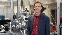
Photo courtesy of Genevieve Martin, ORNL
Hans Christen directs nanoscale material science research at the Center for Nanophase Material Sciences in east Tennessee.
This is a continuing profile series on the directors of the Department of Energy (DOE) Office of Science User Facilities. These scientists lead a variety of research institutions that provide researchers with the most advanced tools of modern science including accelerators, colliders, supercomputers, light sources and neutron sources, as well as facilities for studying the nano world, the environment, and the atmosphere.
Meet the director:
You might say lunar rocks from NASA Apollo missions started Hans Christen on his way to Oak Ridge National Laboratory (ORNL) as the director for the Center for Nanophase Materials Sciences (CNMS). In 1991, Christen, a native of Switzerland, looked to the United States for a postdoctoral position. Many years earlier, his academic advisor had spent time at ORNL examining the Apollo lunar rocks. Through his advisor's ORNL connections, Christen learned of an opportunity to work at the Oak Ridge lab with support from the Swiss National Science Foundation.
Christen came to ORNL with the intention of working one or two years, then returning to Switzerland. But after two years at Oak Ridge, then a stint at an R&D start-up in Maryland, he came back to ORNL to a staff position, working with the condensed matter sciences division. After 13 years here and in a similar position working in material sciences division, he became the division director for CNMS.
"My experience working at ORNL and in industry was good preparation. I've seen CNMS evolve from its very beginning."
CNMS in East Tennessee is now home.
The director's background:
Nanophase Materials
Objects made of nanophase materials are made of the same atoms as the conventional materials. The difference lies in how the nanophase material is assembled of smaller pieces - such as grains, fibers, or even voids - and the number of atoms in each grain, based on its size. The grains are less than 100 nanometers in diameter (a nanometer is one billionth of a meter, approximately the width of three-four atoms; an average human hair is 25,000 nanometers wide). The fewer atoms in nanophase materials means there is a large surface-to-volume ratio of the atoms so that each atom is not very far from a surface or an interface. By manufacturing material with smaller grains, the researcher causes the nanophase material to have different properties. These nanophase materials respond differently to electricity, light, and mechanical stress than conventional materials do. For example, gold is chemically inert, but at the nanoscale, gold becomes extremely reactive.
He describes science as his way of life. "It's a question of curiosity – which is one of the two parts of science. One – it is an absolutely necessary enterprise for our society to come up with solutions," says Christen. "And two, on a personal level, it is a sense of curiosity – trying to figure out how things work. As you watch things, you want to know how they work; you take things apart; you observe. It's the same kind of curiosity that makes you want to find out why materials behave in a certain way."
His need to find answers led him to his love for science and his career. Christen is his family's only scientist. "No one has any relation to science in my entire family. They are schoolteachers, artists, farmers, pastors," says Christen.
The Facility:
The Center for Nanophase Materials Sciences was the first of five DOE Office of Science nanoscale centers, opening its door in 2006. In FY 2016, 601 unique users conducted research at the CNMS facility.
Christen appreciates his role. "The importance of science in furthering our understanding of the world – realizing the impact that can be made by helping others with their work - it is really an honor to make it possible for our own researchers and our users to do their work. It is rewarding to hear from users when they explain how they benefitted from being at CNMS."
"While nano science has been around for 10-15 years, we are now at a cusp," says Christen. The next 5-10 years will allow us to fully integrate our experimental and theoretical capabilities – enabling real breakthroughs."
Material scientists are making great strides towards their research goal: precisely synthesizing a desired material from the atoms of common elements. This enables predictive material science – the knowledge to predict how the material will behave before the researcher makes the structure. Every atom would be chosen for its specific properties and placed precisely to build a 3-D nano structure. Advanced microscopy will be able to see where every atom sits and what every atom does. From a computational perspective, it will be possible to understand the role of every single atom in a nanostructure that we create.
"This will be possible and it will happen. It is a very exciting time," says Christen.
Typical day:
The majority of the CNMS staff are active researchers. They spend half of their time conducting their own research; the second half is spent working with the users from outside institutions to conduct research at CNMS. "What we have is a working web of capabilities that play together and give the user much more than just a piece of equipment – we provide the missing pieces for the user from the synergy of our in-house experts," explains Christen. The interaction of staff and user breeds a climate of natural feedback to advance the work.
Sharing of equipment is common; all equipment can be accessed by all users. An additional benefit is the integration into a national lab and proximity to a research university. "We are a gateway to access other equipment at ORNL. We have researchers with joint appointments with other ORNL divisions and with the University of Tennessee. In addition to the large user community, we have student interns from many universities here for a short time," says Christen. "It creates a very lively environment and gives an opportunity to train the next generation of researchers."
Typical experiments:
Users come to CNMS for synthesis and fabrication, imaging, and computational abilities.
They come to synthesize polymer samples or make structures in which fluids flow, then continue their work at their home institution.
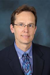
Photo courtesy of Genevieve Martin, ORNL
Hans Christen is the director of the Center for Nanophase Material Sciences, located at Oak Ridge National Laboratory.
They also come to prepare their materials for studies at another ORNL facility, the Spallation Neutron Source. One technique available at CNMS is selective deuteration - replacing some of the hydrogen atoms in a polymer with a different isotope, i.e., deuterium. The deuterium does not change the response of the material but it does change how the material appears to neutrons, helping the researchers when they examine the material via neutron scattering.
And they come for imaging and characterization capabilities, to understand the structure of a defect in their samples, for example. They often use scanning probe microscopes, a technique for which CNMS staff have developed and licensed a clever engineering approach: oscillate the tip of a scanning force microscope at a whole range of frequencies, a sensitive and quantitative technique.
CNMS computer scientists also help users convert their computational projects to take advantage of high performance computation resources available at the Oak Ridge Leadership Computing Facility.
Best advice for a future director at CNMS:
"Be open and learn," advises Christen. "The center works as a team and I enjoy being part of that. My favorite part of the job is knowing that we do something of relevance; we help users, we contribute to finding solutions for society."
In Fiscal Year 2016, CNMS and the other twenty-six user facilities welcomed 33,754 researchers - from academic, industry, and government laboratories in all 50 states and the District of Columbia – to perform new scientific research. For details on the Office of Science User Facilities, go to: https://science.energy.gov/user-facilities/.
Please go to Profiles of User Facilities Directors to read more articles on the directors for the Office of Science user facilities.
The Office of Science is the single largest supporter of basic energy research in the physical sciences in the United States and is working to address some of the most pressing challenges of our time. For more information please visit https://science.energy.gov.
Sandra Allen McLean is a Communications Specialist in the Office of Science, sandra.mclean@science.doe.gov.